System overviewEngineered around your production requirement
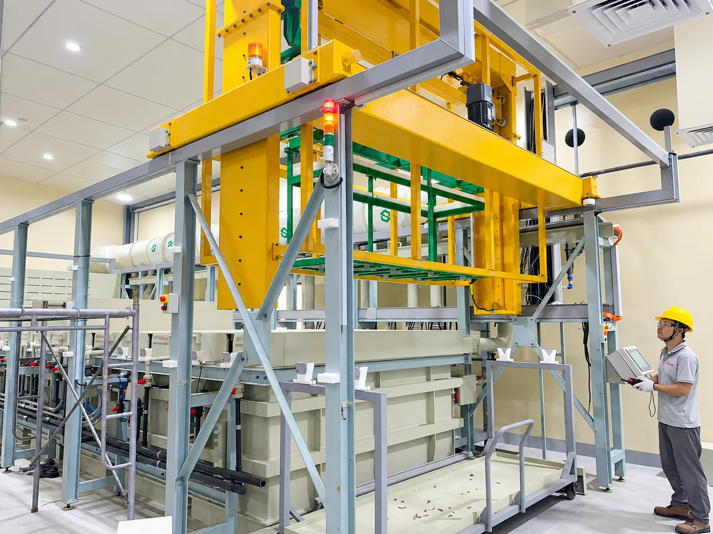
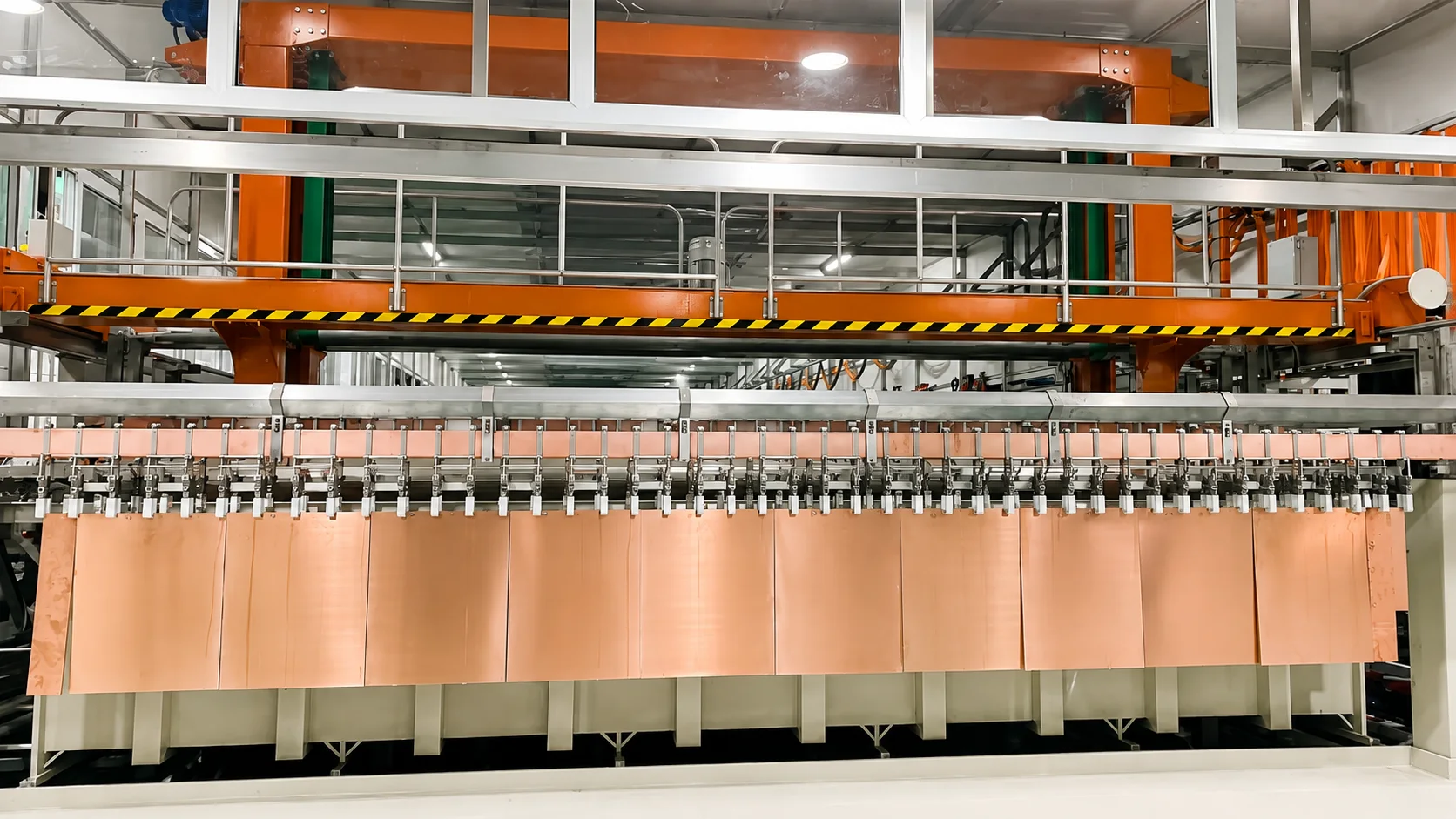
Hole Filling Electroplating systems are designed for advanced PCB, HDI and semiconductor applications requiring reliable copper via filling, microvia filling and high-density interconnection.
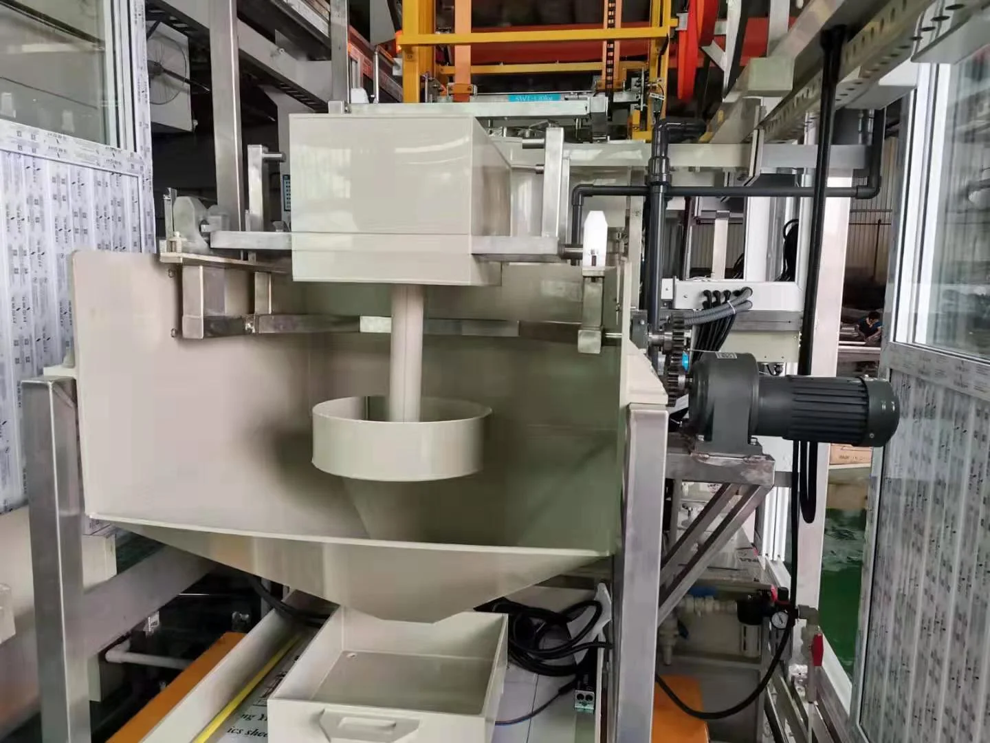
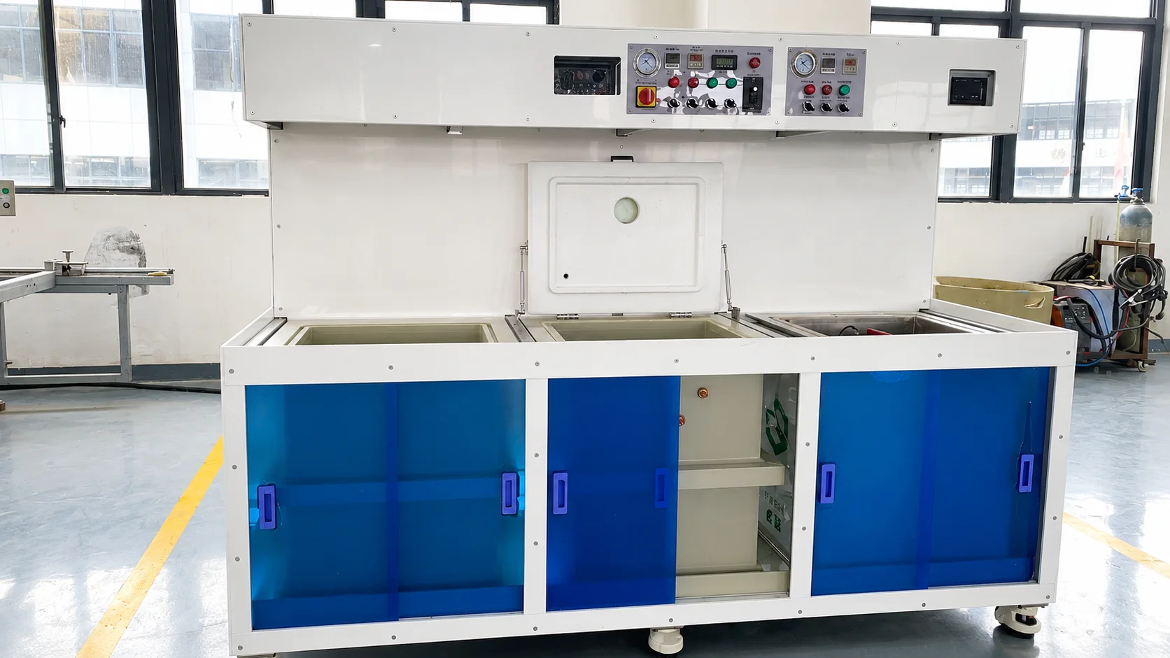
ES-PRO provides customized copper electroplating solutions with optimized current distribution, electrolyte circulation, filtration, temperature control and chemical management to achieve void-free filling, uniform copper deposition and stable plating thickness. The system can be configured for blind vias, through holes, microvias and other high-aspect-ratio features according to board design, hole geometry, production capacity and process requirements.
Typical process architectureProcess flow
LoadingCleaning / DegreasingMicro-etchingRinsingActivationCopper Seed / Electroless CopperRinsingHole Filling ElectroplatingRinsingSurface FinishingFinal RinsingDryingInspectionUnloading
The displayed flow is an engineering reference. The final sequence, chemistry, dwell time and control points are confirmed for the customer’s process.
ApplicationsWhere this system fits
Hole filling electroplating is widely used in advanced electronic manufacturing where high-density interconnection, reliable conductivity and void-free copper filling are required.
HDI printed circuit boards
Microvia and blind via filling
Semiconductor substrates
IC packaging substrates
Through-hole copper filling
High-density multilayer PCBs
Automotive electronics
Communication and high-frequency electronic products